The process would surpass conventional lithography machines, which are the main way today of making the semiconductors used in most electronics.
When a lithography machine etches a chip circuit, the laser strikes the material vertically. If light goes sideways, it causes uncontrolled damage, particularly in soft materials such as lead halide perovskites.
Advertisement
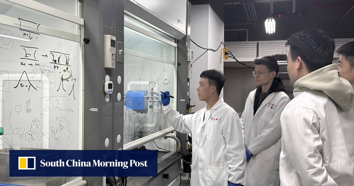
Lead halide perovskites are a very promising area of semiconductors because of their exceptional optoelectronic properties in two-dimensional crystal lattice form but they are difficult to machine precisely due to their soft and unstable nature in 2D.
However, the new process creates lateral microstructures in these perovskites in a controlled way, adding a new dimension that could lead to revolutionary performance improvements in semiconductors.
Advertisement
The international team said it had developed a novel “self-etching” technique that enabled the world’s first fabrication of intricate structures in superthin perovskite materials without damaging their structure.