
Loading . . .
Working in chip innovation was not always the plan for Min Cao, vice-president of pathfinding at Taiwan Semiconductor Manufacturing Company (TSMC).
Cao had dreamed of a career in physics, but after graduating from Stanford University at the end of the cold war, an abundance of out-of-work physicists meant he cast his net more widely. His desire to understand how the world works led him to the rapidly developing field of microchips.
“There are still a lot of mysteries,” says Cao, whose work on chip performance continues to push the limits of physics. “It’s getting harder, but it doesn’t mean we are going to stop.”
Only three companies in the world — Intel, Samsung and TSMC — are capable of mass producing chips powerful and small enough for today’s advanced mobile technologies.
With parts of transistors reaching atomic levels of scale, engineers are having to come up with increasingly innovative ways of ensuring progress, such as vertical, tower-like construction and rethinking the way chips are packaged. Many believe bundling together chips with different functions is where future semiconductor battle lines will be drawn.
Some of the newest smartphone chips, such as those in the iPhone 15 Pro, are manufactured with what is called a “3 nanometre” process — a name given to a generation of processors with the smallest transistors. Although this no longer references their physical dimensions, it does allude to the shrinking scale of their components. These tiny switches, which control the flow of electrical signals inside every digital device, are the workhorses of microprocessors and the basic building blocks of modern electronics.
Driven by demand for increased computing power, the scaling of chips over time has for decades followed Moore’s Law, the observation by Intel co-founder Gordon Moore that the number of transistors on an integrated circuit would double every two years. But progress has slowed, with doubling now closer to every three years.
The current 3nm process has suffered from poor yield rates — the proportion of chips produced that can be sold to customers — and only marginal improvements in efficiency.
But far from being at the end of the transistor innovation journey, Intel’s Ben Sell, vice-president of technology development, suggests we are right “in the middle” of it. What is particularly exciting, he says, is that chip innovations discussed “for decades” are now being seen in devices on the market.
But success is not guaranteed — and the stakes are high. Global chip sales hit well over $500bn last year and semiconductors could become a trillion-dollar industry by the end of this decade, according to consultants McKinsey.
“That’s like getting to GDP scales of things that the companies are competing over,” says Jeff Koch, analyst at SemiAnalysis, an independent research company specialising in semiconductors and AI.
The technological reputation and financial standing of companies and governments depends on the right bets being made.
TSMC, with its market capitalisation of $575bn, dominates Taiwan’s economy and the global market for the world’s very smallest cutting-edge chips.
That is something the Biden administration hopes to change with its Chips Act, pledging $52bn of incentives to encourage companies to base fabrication plants on US soil. But many experts believe the erosion of US chip manufacturing over a number of decades has made it hard for the country to regain global competitiveness.
China is also entering the race, with the country’s biggest chipmaker SMIC expected to make next-generation smartphone processors as early as this year — despite US efforts to restrict Beijing’s chip advances through export restrictions on specialist equipment.
Nvidia and Advanced Micro Devices (AMD) are also battling for technical supremacy and market share in the field of AI chips, given the soaring demand for the processors that power OpenAI’s ChatGPT and similar apps.
AMD revealed a raft of technical advances in December, including packing 153bn transistors and 192 gigabytes of memory into its new MI300 chip, in a bid to take on the world’s most valuable chip company, Nvidia. Last week, Nvidia’s market value soared to $2tn, leapfrogging Amazon and Alphabet to become the third most valuable US-listed company, behind Microsoft and Apple.
AMD, meanwhile, brought in revenues of $23bn in 2023 and expects to sell $3.5bn-worth of its latest chips this year. It is the second-most-valuable semiconductor company in the US — overtaking Intel in 2022. Intel is also bidding for a place in the AI landscape, announcing it will be building Microsoft’s high-end chips.
Chip construction
A diminishing number of companies have been able to keep pace in the race to build the most advanced smartphone chips in recent years. The design and manufacturing processes have become extremely long, complex and costly, requiring ever more specialist equipment and knowledge.
Advances take years of experimentation and require staggering levels of R&D spending.
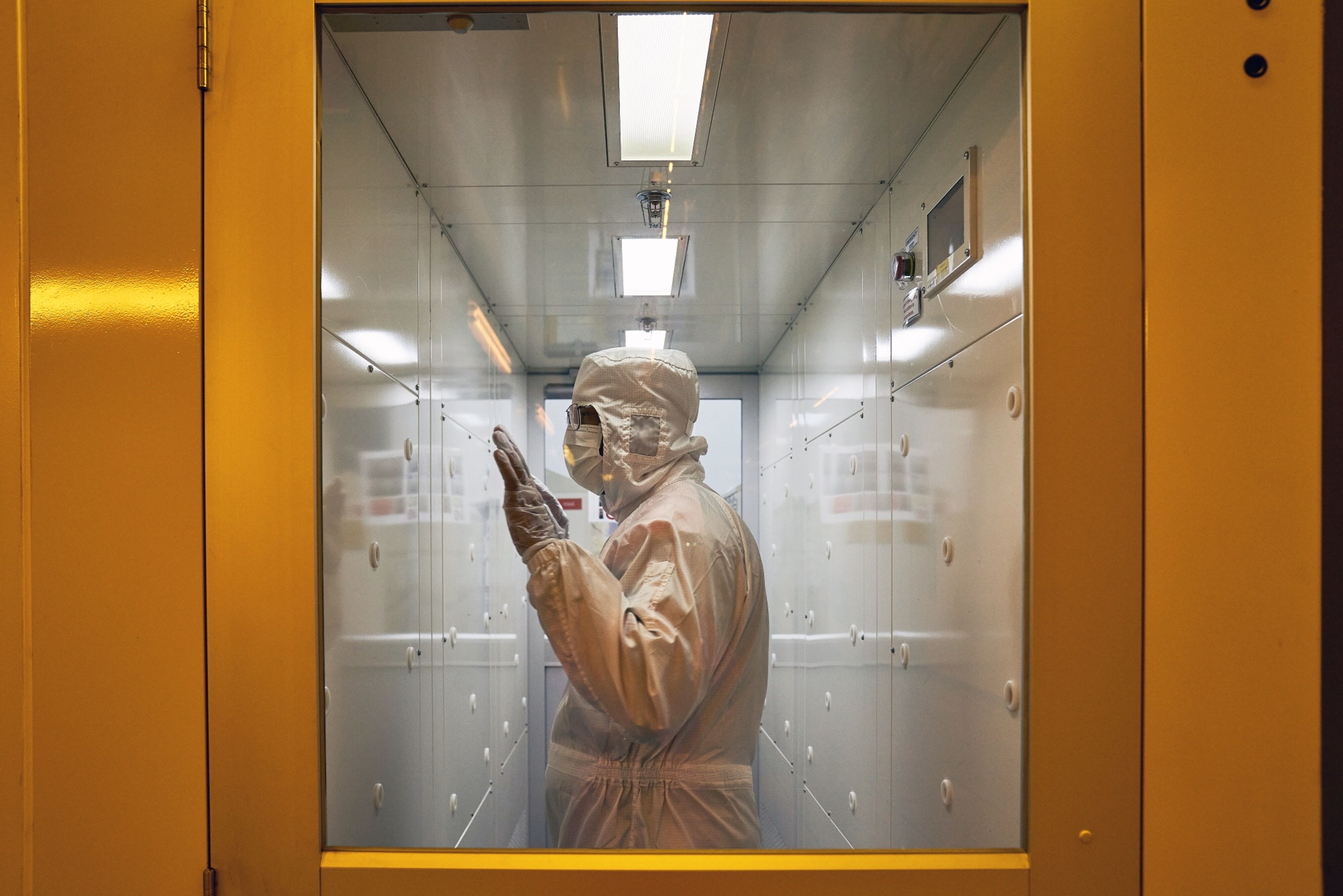
Working at nanoscale is also full of jeopardy. Precision, repeatability and cleanliness are some of the biggest challenges, says Sell, explaining that any particle, even those smaller than a bacterium, could “kill” a chip on contact.
Inside chip fabrication plants, more than a thousand precisely controlled steps create each integrated circuit, layer by layer. Every time a new generation of chips is developed, these stages all need to be reviewed, says Chris Auth, director of advanced transistor development at Intel. “You have to be pretty fearless about trying new things and saying, ‘Hey, let’s just see what happens’,” he adds.
A new chip generation also requires new tools and processes, says TSMC’s Cao. The transistor advances in the next 2nm chips mean some elements need to be built laterally, rather than vertically, bringing extra challenges, he adds.
“There are a lot of things happening in the same node [generation], even though we give them just a simple number, like 2nm.”
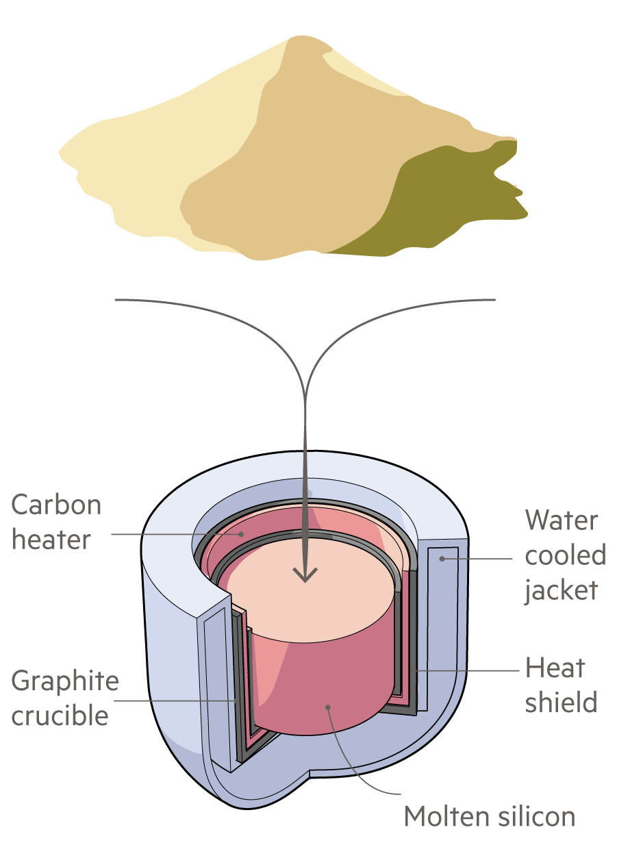
But before any of these complex steps of fabrication begin, the base of the chip is still made with a simple, common substance called silicon, extracted from sand or quartz.
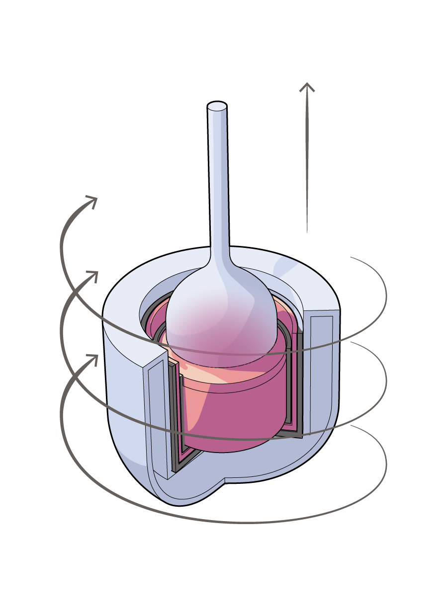
The chip manufacturing process

1Silicon is extracted from sand and purified. It is then added to a crucible and heated until molten
2The crucible is rotated at speed while a solid piece of ‘seed’ silicon is pulled up using a rod
3The result is a silicon ‘ingot’ or ‘boule’. The largest have a diameter of 300mm
4The silicon boule is sliced into discs, known as wafers, and polished to a mirror-smooth finish


5Ultraviolet light, projected through a stencil, transfers tiny patterns onto the wafer
6Many thin films of materials are added and etched away using these intricate patterns as a guide
7The wafer is hit with ions, or charged atoms, to make areas more conductive or insulating
8Hundreds of stages of layering build up the chip’s components. Metal wiring completes the circuit

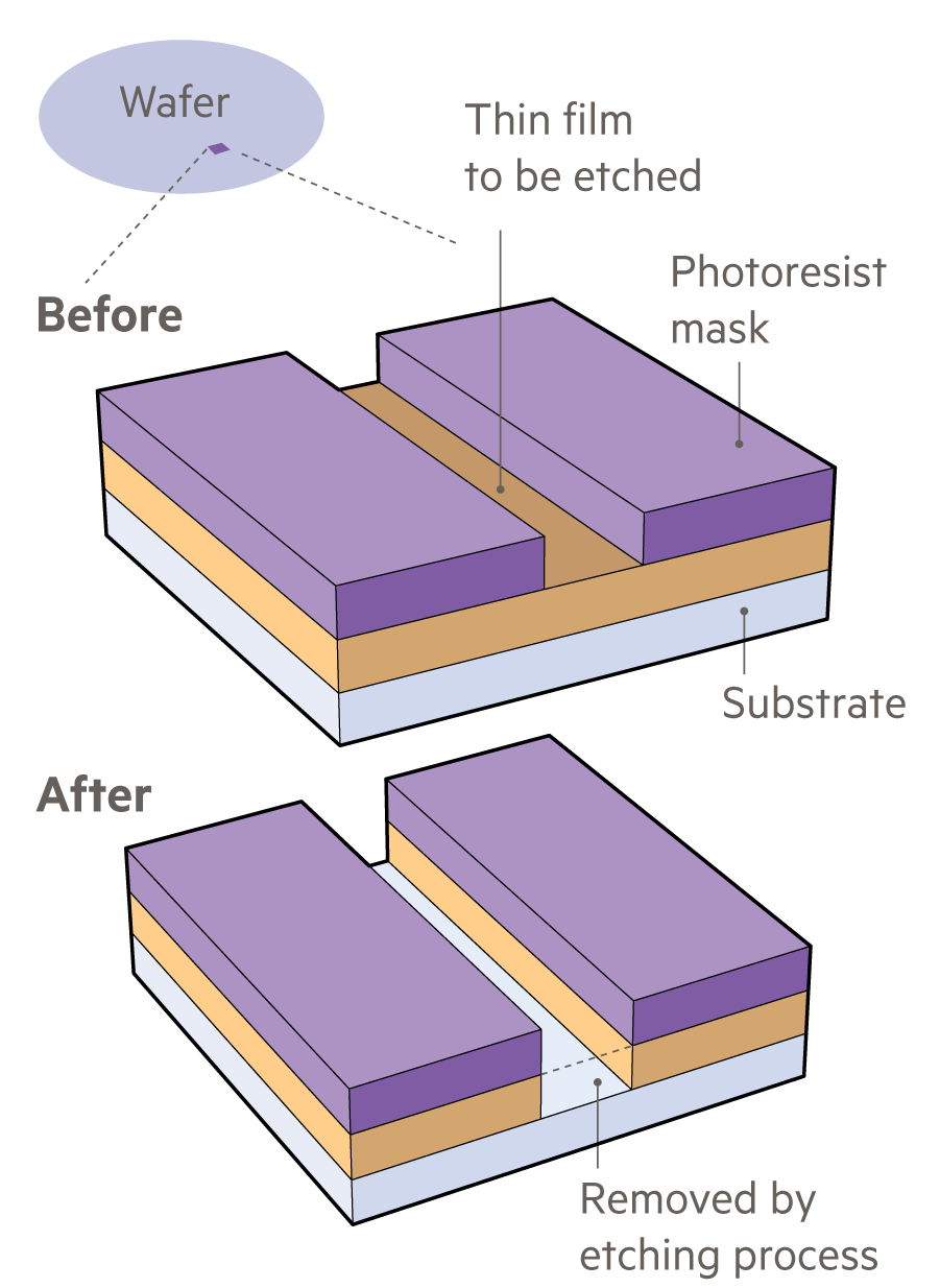


Creating the tiny components for a chip’s circuits requires cutting-edge equipment: machines that can transfer microscopic patterns on to each wafer using a process called photolithography.
For the smallest chips, multi-million-dollar machines made by a single Dutch company, ASML, use extreme ultraviolet light to create these fine stencils. The machines are the size of a bus, but so accurate they could direct a laser to hit a golf ball as far away as the Moon.
Every stage of this process requires “PhD thesis level of knowledge”, says Koch.
A wafer full of chips can be worth thousands of pounds when it leaves a top fabrication plant.
Rethinking power and packaging
While leading manufacturers are hoping the 2nm chip will solve many of the 3nm generation’s problems, the limits of scaling mean engineers are already developing alternative ways of getting more power and efficiency out of the same space.
Building on current 3D designs, engineers plan to stack transistors on top of each other, rather than cramming them in side-by-side.
“You’re really starting to expand that third dimension, which is something that hasn’t been used in the first 60 years of transistor technology,” says Intel’s Auth. “[When] you build skyscrapers, you start to run out of the ability to shrink things laterally, so you start to build up and that’s what we’re doing.”
The way chips are packaged is also going upwards. The growing field of “advanced packaging” — how chips are bundled together to boost capability as well as reduce cost — is moving towards stacking chips to improve performance and better use available space.
This pivot to vertical design and development is “kind of a big deal”, says Koch of SemiAnalysis, because it is the first time the industry has acknowledged that it’s running out of horizontal options. “We’re slowing down in one direction, but speeding up in another,” he says.
Cao says advanced packaging is where major progress can be made — a field in which TSMC is heavily invested. “There are a lot of different configurations that can be used . . . a lot of things are happening in this field.”
Packaging developments have paved the way for another shift in semiconductor architecture: “chiplets”.
Engineers are moving away from building an entire microprocessor on a single piece of silicon — the monolithic “system on a chip” — and towards multi-chip modules (MCMs). These MCMs see groups of chips with different functions built on separate pieces of silicon and then bundled together to work like a single electronic brain.
Many believe chiplet manufacturing is the only way to keep Moore’s Law alive in the longer term. Intel, AMD and Apple have already launched products, while others, like Nvidia, have indicated they have them in development. AMD’s latest MI300 employs modular architecture.
The companies investing in MCMs say one of their key advantages is flexibility — they can be adapted for different customers because makers can swap in chiplets depending on requirements. They also offer manufacturers the option of mixing older and newer designs and upgrading elements incrementally, rather than overhauling a chip’s entire system at once.
This means companies can “react quickly”, says Auth. “If the market wants more of one thing or another, you don’t necessarily have to change the GPU [graphics processing unit] or the CPU [central processing unit], you can just change one component.”
This can lead to improved performance overall, he says, because you can “pick and choose what provides the best outcome for the end customer”.
One of the things that has been holding back the wider adoption of chiplets is the lack of standard rules for interfaces, which means it is not yet possible to mix and match products from manufacturers. But this remains the long-term goal for many companies, including TSMC, Intel, Samsung, AMD and Google, who have formed a consortium in the hope of doing so.
A number of chipmakers are hoping further performance gains can be made through a major rethink of how chips get their power.
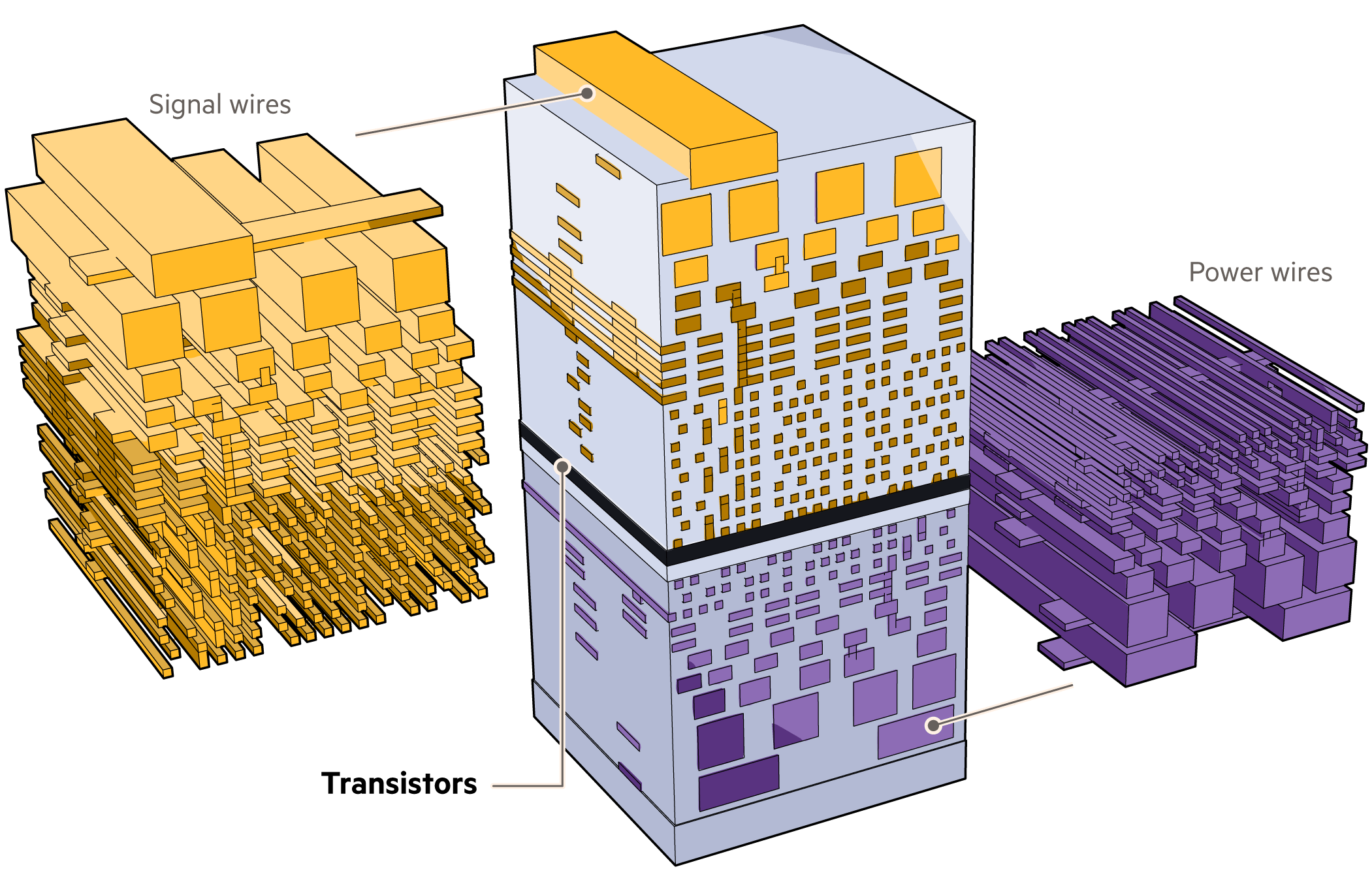
Upcoming 2nm designs include separating the metal wiring that joins a chip’s elements from those that bring in power — something never done before. Power wires will move from the top (front), to the bottom (back side) of the chip, sitting below the transistor layer, rather than above. The interconnects will stay put. Early tests show this direct route for power and reduced tangle of wires results in greater efficiency.
Rethinking wiring could improve chip efficiency
In traditional chip architecture, power and signal wires are integrated above the transistors, causing bottlenecks
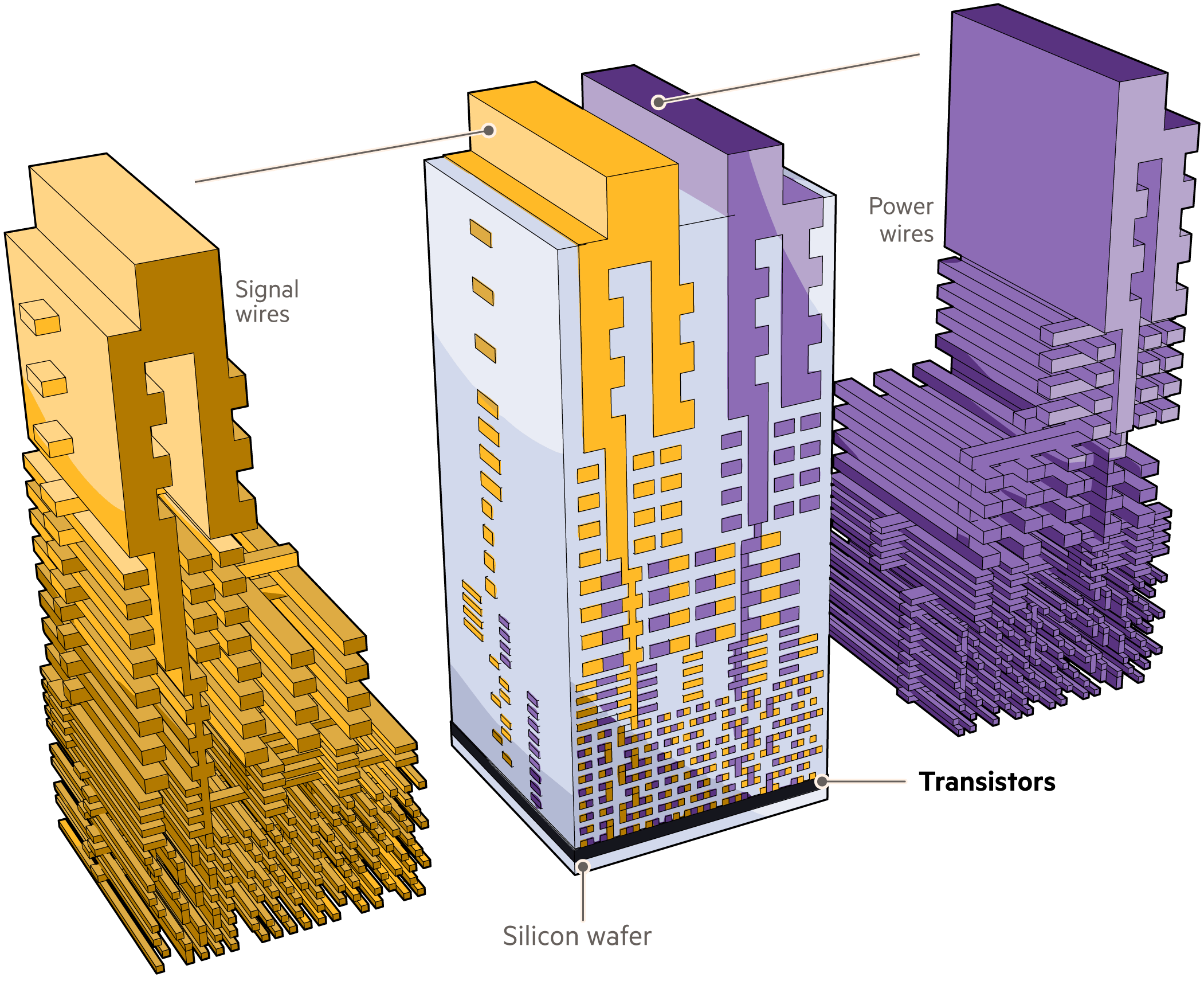
With back-side power architecture, power wiring is moved below the transistors, separating it from the signal interconnects and improving efficiency
Alternatives to silicon may also be seen within the decade. High-mobility or 2D materials, such as graphene, which allow electrons to move around quickly, could pave the way for “faster switches” and a leap in capabilities, says Sell.
“The periodic table has a lot more elements to work with, so there’s plenty of room for us to innovate,” he adds.
Another emerging field is photonics, where photons, the building blocks of light, are used in place of electrons to carry data at higher speeds. Companies, including TSMC, are currently experimenting.
Although nothing in chipmaking is ever certain, the accelerating demand for AI, illustrated this month by Nvidia’s bumper results and bullish forecasts, will mean no shortage of incentives for chipmakers to continue increasing computing power.
“It’s so integral to what we do in our everyday lives and I think we take it for granted,” says Intel’s Auth, reflecting on the leaps in science enabling chip development. “I’m excited to see what we can do over the next 20 years.”
Cao is equally confident his team of TSMC engineers can continue to be pioneers, developing new generations of chips at a “regular pace” well into the future. The company’s customers demand it.
“It stops when no one’s asking for it,” he says. “And that is not the case.”